Background
Picking a translucent material for a lamp shade, a diffuser panel, or a display cover usually comes down to guessing which one looks best. Hold the sample up to the light, squint a bit, maybe hold it next to another sample, and “yeah, this one looks about right.”
The trouble is two materials that look identical under room light can behave completely differently once they’re backlit. Surface finish, thickness and internal structure all affect how light moves through the material, and renderings can only get you so far. At a certain point, you have to see it with your own eyes.
So I built a test platform, so that every CMF decision after that would rest on a fixed process.
Requirements
Four optical properties, each directly relevant to product design decisions:
| Property | What It Tells You | Why It Matters for Design |
|---|---|---|
| Transmission | How much light gets through the material | Brightness of backlit displays, LED indicator visibility |
| Diffusion | How evenly the light scatters after passing through | Hotspot elimination, uniformity of illuminated surfaces |
| Reflection | How the material surface bounces incident light | Surface finish selection, glare management |
| Luminance Distribution | Brightness variation across the illuminated area | Visual comfort, light guide performance |
Beyond the measurement goals, I had a handful of practical requirements, and they turned out to weigh just as much as the optical ones. Repeatable positioning came first: if I can’t place samples at consistent distances from the light source, nothing I measure afterwards means anything. Adjustable brightness mattered because a material at 10% and that same material at 100% are two different objects, so the source has to cover the whole range. Ambient light control was non-negotiable, since optical measurements taken in a sunlit room are mostly noise. Quick sample swapping, because at five minutes per changeover I would never run enough comparisons to learn anything. And visual output, because seeing two materials side by side is half the point.
Design & Build
Platform Architecture
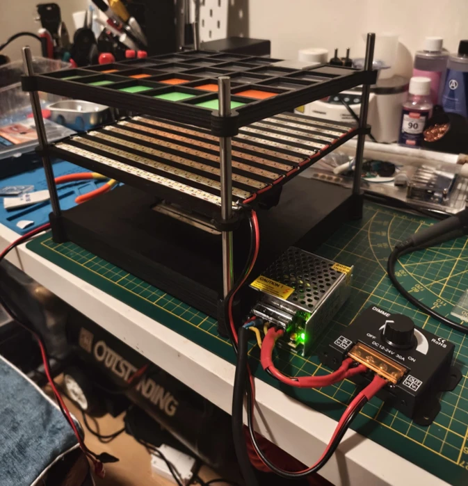
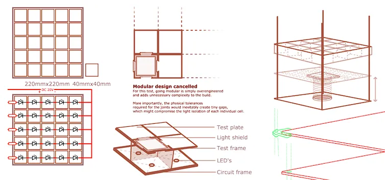
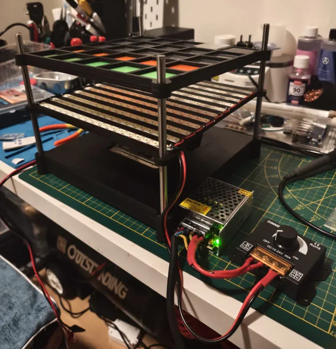
The platform is a vertical measurement stand: light source at the bottom, adjustable sample stage in the middle, observation from above. The layout is basically a stripped-down optical bench: nothing I didn’t need, nothing that gets in the way.
Final 3D Render
Concept Sketch
Key Components
- Light source: LED strip, goes from barely glowing to full output.
- Lift stand: The height adjustment lets me precisely control the distance between the light source and the material.
- Frame: Laser-cut structural panels, spray-painted matte black and absorbs stray ambient light and kills internal reflections.
- PWM Controller: Use PWM to control the LED strip’s dutycycle to adjust its brightness.
- Power delivery: Oxygen-free copper wire 0.5mm², comfortably above the 2A the strip draws.
Fabrication Process
 STEP 1: 3D Modeling
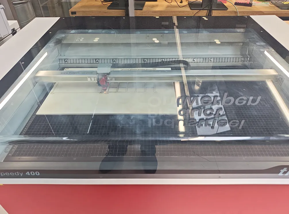 STEP 2: Laser Cutting
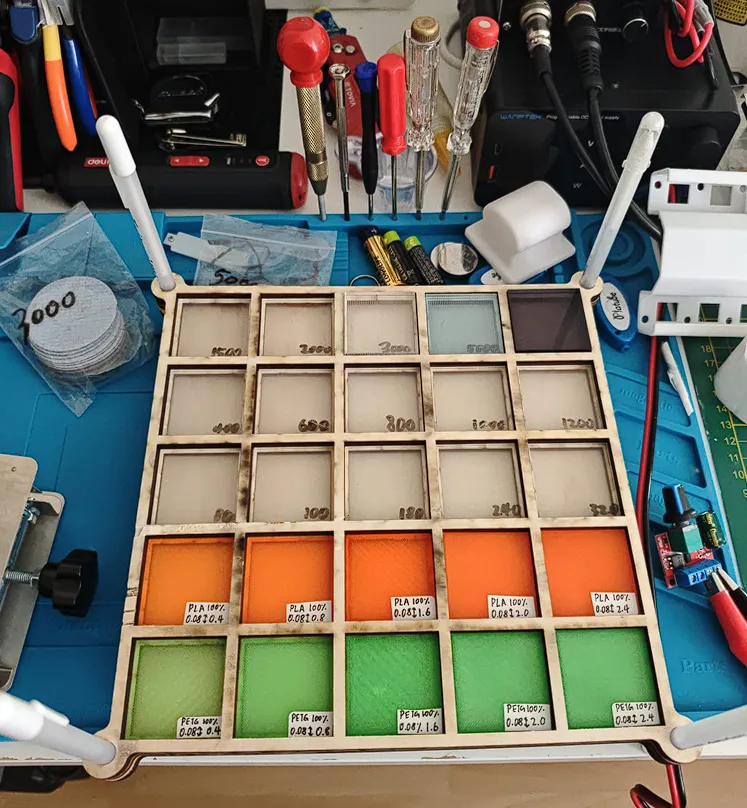 STEP 3: Test Build
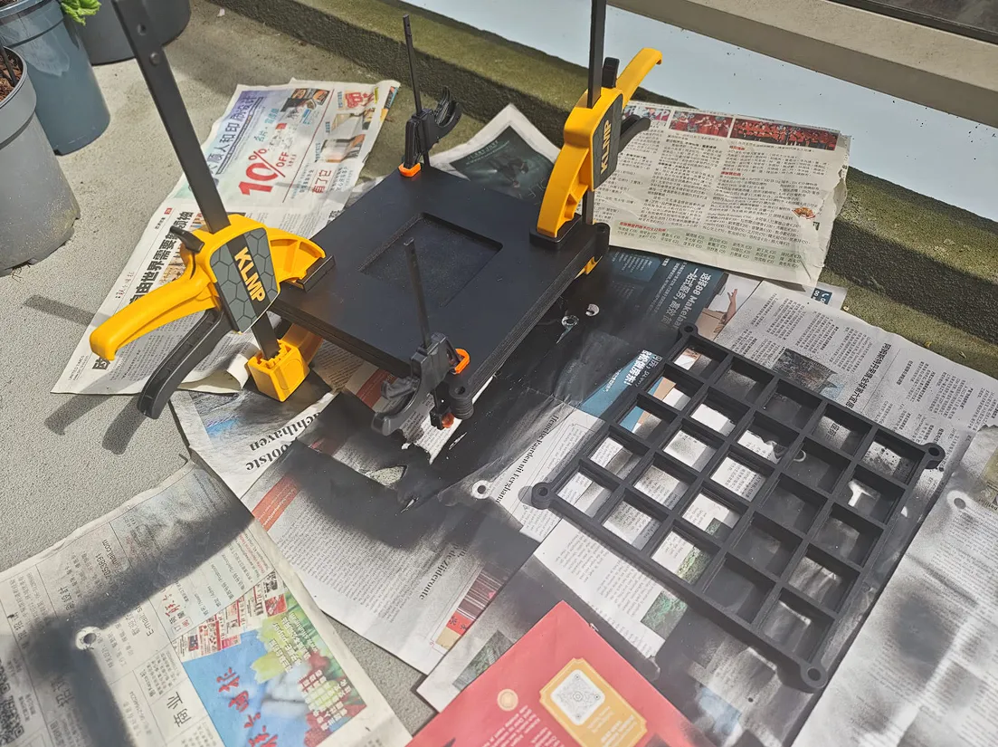 STEP 4: Surface Finish
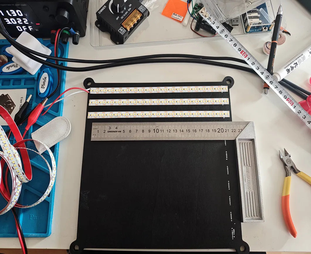 STEP 5: Subassembly
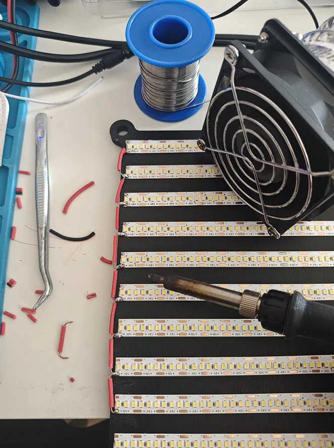 STEP 6: Circuit Soldering
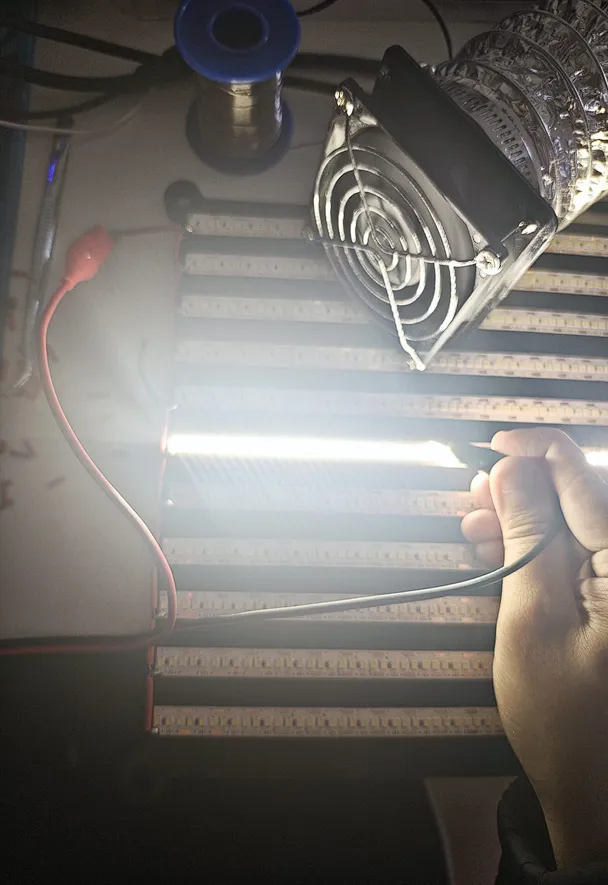 STEP 7: Circuit Verification
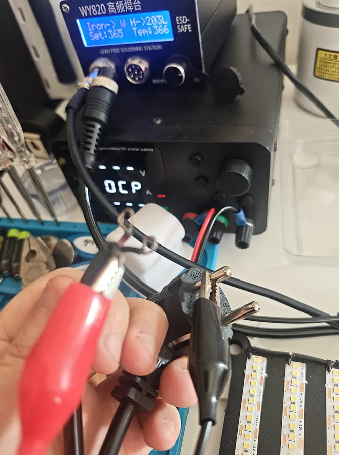 STEP 8: Polarity Check
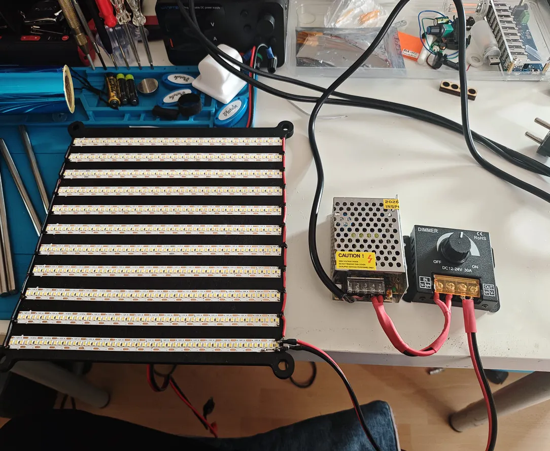 STEP 9: Final Assembly
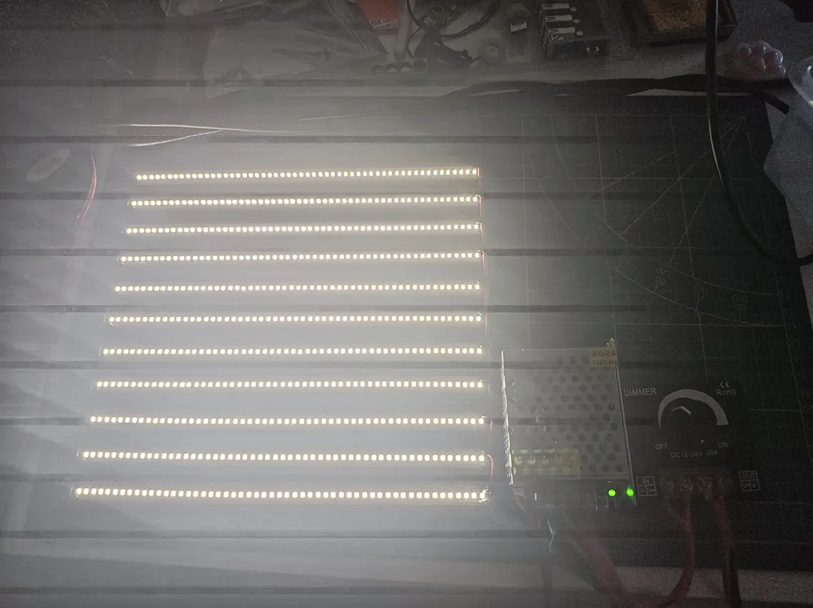 STEP 10: Circuit TestingSTEP 1: 3D ModelingSTEP 2: Laser CuttingSTEP 3: Test BuildSTEP 4: Surface FinishSTEP 5: SubassemblySTEP 6: Circuit SolderingSTEP 7: Circuit VerificationSTEP 8: Polarity CheckSTEP 9: Final AssemblySTEP 10: Circuit TestingSTEP 1: 3D ModelingSTEP 2: Laser CuttingSTEP 3: Test BuildSTEP 4: Surface FinishSTEP 5: SubassemblySTEP 6: Circuit SolderingSTEP 7: Circuit VerificationSTEP 8: Polarity CheckSTEP 9: Final AssemblySTEP 10: Circuit Testing
Material Testing
I tested a range of translucent and transparent materials that show up frequently in product enclosures, diffusers, and light guides:
Test Materials
| Material | Type | Key Characteristic |
|---|---|---|
| Translucent PLA | 3D-printed | Layer-line scattering, cheap for prototyping |
| Translucent PETG | 3D-printed | Better clarity than PLA, stronger layer adhesion |
| Acrylic Sheet | Laser Cut | Great optical clarity, scratch-resistant, lots of surface finish options |
| AB Epoxy Resin Plate | Cast resin | High transparency, smooth surface, glass alternative |
| PC Light Diffuser Sheet | Extruded polycarbonate | Purpose-built for diffusion, prismatic surface texture |
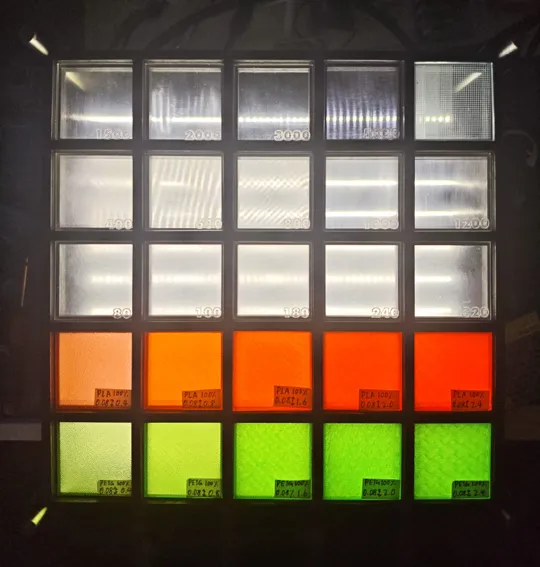
Each material went through multiple configurations: different thicknesses, different surface finishes, different distances from the light source: so I could see how material choice actually affects the final visual output.
Controllable Variables
The whole point of building this thing was to change one thing at a time. Systematic A/B testing is only possible if you can lock every variable except the one you’re studying.
- Light Intensity : set via the PWM controller, from barely visible to full blast
- Material Type : PLA, PETG, Acrylic, AB Epoxy, PC Diffuser
- Material Color : Natural, white, and tinted variants of PETG and acrylic
- Material Thickness : Single layer, stacked layers, different sheet gauges
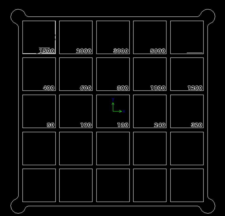
- Surface Finish : Raw print, sanded (80–5000 grit), polished, textured
- Diffusion Distance : The gap between light source and sample, adjusted via the lift table
Design Iterations
The platform didn’t arrive fully formed. I did three iterations, and each version fixed something the previous one got wrong.

| V1: Single LED | V2: LED Strip | V3: LED Strip + PWM | |
|---|---|---|---|
| Method | Hand-soldered | Copper foil tape | PWM controller |
| Issues | ✕ Soldering too slow | ✕ Tape unsuitable for 2A | ✓ Brightness adjustable |
| ✕ Light effect poor | ✕ No brightness control | ✓ Diffuse reflection from dark surfaces | |
| Verdict | ✕ Discarded | ✕ Discarded | ✓ Final |
V1: Single LED: Manual Solder
I was planning on hand-soldering individual LEDs to the board. It was the obvious first approach, and it was wrong in exactly the ways you’d expect.
- Issue: Hand-soldering twenty LEDs is tedious and inconsistent. Each joint has slightly different resistance, so each LED glows a tiny bit differently. For a test platform, “tiny bit differently” is fatal.
- Issue: A single-point light source creates uneven illumination across the sample. If the light isn’t uniform to begin with, you can’t tell whether the diffusion pattern you’re seeing is from the material or from the source.
V2: LED Strip, Copper Foil Tape
I swapped the individual LEDs for a uniform LED strip and used copper foil tape for the electrical connections. Better, but new problems.
- Issue: Copper foil tape is convenient and looks clean, but it is thin, and every connection in it is adhesive rather than metal. That is not a dependable way to carry 2A: the copper may survive it, the joints are where the heat collects. I worked the numbers through and realized this was a fire hazard waiting to happen.
- Issue: Fixed brightness. No matter what material or distance I was testing, the light output was the same. Different scenarios need different illumination levels, and I had no way to adjust.
V3: LED Strip + PWM Controller (Current Version)
This is the one that stuck:
- Upgrade: Replaced the tape with oxygen-free copper wire 0.5mm², which puts real metal at every joint and sits comfortably above the 2A the strip draws.
- Upgrade: PWM controller for full-range brightness adjustment. Now I can test at any level in between and get the same reading every time.
- Upgrade: Painted the interior frame matte black. Ambient light and internal reflections had been silently contaminating every reading.
Result
The finished design gives me a reliable, repeatable environment for comparing how materials handle light. Side-by-side material comparison under identical lighting retires the old “I think this one looks better”. I can work through surface finish evaluation and see what sanding, polishing or texturing does to the way light moves through. I can run a thickness versus transmission analysis and find out what doubling the sheet actually costs in brightness. I can do controlled brightness sweeps and watch a material across the full dimming range. And every run leaves visual documentation of the light distribution that I can pull up on the next project.
What I Learned
Beyond the CMF data, building this platform drilled in a few principles that apply to pretty much any design-build project:
Current ratings are important: the copper tape was a concrete reminder that prototyping materials have to be judged against their actual electrical loads, and that a clean-looking build means nothing if the wiring is undersized. Your environment is part of your instrument: optical measurements live and die by ambient light control, and twenty minutes with a can of matte black paint improved measurement consistency more than any other single change. Isolate one variable at a time, or you are just guessing, because being able to change material, thickness, finish or distance independently is exactly what turns holding things up to a lamp into an experiment. And tools pay for themselves across projects: the platform felt slow to build, but every CMF decision involving translucent materials now starts from real measurements instead of squinting and hoping.
Future improvements
Replace manual PWM control with calibrated digital control. The setup relies on a manually adjusted PWM controller, which is fine for exploratory testing but leaves some variation in light intensity between measurements. A microcontroller could generate precisely defined PWM signals and store repeatable intensity settings, so the same lighting conditions could be reproduced across tests. That would make the data more reliable and comparisons between materials more rigorous.